Every 8-bit computer needs some kind of output display, whether this is a LCD display, or a 7-segment display, it needs some way of displaying data to the outside world. Wouldn't it be cool to have a pretty RGB LED display as a way of not only showing the output of computation, but to act as a screen for showing animations, even playing simple games? At the very least it would be cool to have a kind of "RAM visualizer" to show the contents of RAM for debugging purposes.
With that in mind, I recently came across a post on the timing for WS2812 LEDs, part 1 and part 2, in which the blog post author Tim sets out the limits of the WS2812 LED protocol and shows they are rather flexible and not as stringent as the official datasheet suggests (i.e. see here for WS2812b datasheet or here). Further he suggests a way of controlling LED strips with a simple timing cycle, encoding either a 0 or a 1 bit, like so:
Tim then goes on to write some assembly language to control WS2812 LED strips using this quantised approach. This is interesting of itself, but it also inspired me to wonder if I could encode bits using hardware (TTL chips, naturally...), and then provide a continuous stream of bits from a byte, and then loading in the next byte from memory at the appropriate time.
Out "0" and Out "1" Logic
First of all we need, some logic to handle the timing of the cycles (t0, t1, etc), and take the given data-bit, i.e. 0 or 1, or produce the out "0" and out "1" signals in the figure above. Having three cycles is a little inelegant when we are using binary, wouldn't it be easier if used 4? Tim's blogpost reassures us that indeed we can play fast and loose and extend the time between bits. Therefore if we use a 4-bit counter, we can use the lower 2 bits for the cycle-timing, and we can construct a logic table using these two bits (Qb and Qa from the counter outputs) and the data bit, like so:
Clearly we can construct this with some NOT gates, some AND gates and some OR gates! That's a lot of gates. However with a bit of thinking, I realised I could construct this logic table from only 4 NOR gates, if I used the NOT of the data signal (!DATA). The shift register (
74LS165) I will use has the NOT of the output bit conveniently on a pin to use, saving me a logic gate. More conveniently, the
74LS02 ic has 4 NOR gates on it, so we can capture all our signal shaping-logic with a signal chip, i.e.:

The eagle-eyed will notice that the final NOR gate functions as a NOT gate. This is of interest as we can use this final gate potentially as a way of enabling and disabling the output. If we connect one of the final-NOR gate inputs to a control signal, then we will only have output '1' if the control signal is 0 and the other NOR input is 0 (else it will output '0'). This will be useful for providing a mechanism to have an enable/disable signal and thereby be able to provide a reset pulse for the LED strip, rather than a continuous stream of data.
Streaming bits
Now we need a way to change the data-bit that feeds into the NOR logic. Ideally we want to load a byte into a shift register, let the NOR logic shape the pulse for the WS2812 LEDS, shift the next bit out, count the number of bits shifted and then load in the next byte to the shift register - we will presumably want to retrieve these bytes from some memory, so at some point we'll want increment a memory address too! Quite a few things for us to think about, let's start with a table that captures all this functionality, just by counting from 0 to 31:

Above is the timing diagram for shifting a byte, incrementing the RAM address and loading in a new byte from memory. QA-QF are the binary counter outputs we get from connecting the 4-bit counters together on a
74LS393 IC to produce an 8-bit counter. The table is divided by the black horizontal bars, which show each of the 4 cycles of the NOR-gate timing cycle (i.e. the 4-cycle encoded bit sequence that is sent to the LED strip). You'll notice that the SHIFT for the shift register register occurs in the middle of this 4-cycle sequence (
blue lines). If we're changing the data-bit as the input into the NOR-gate halfway through the sequence, won't this cause problems with the output? Actually no, the output signal of the NOR-gates at this point in the timing cycle always outputs a 0, regardless of the data-bit, so this is a safe place to change the data-bit (and is , conveniently done use the rising edge of QB as the shift clock). At counts 30 and 31 we have shifted all the bits out of the shift register and the serial in pin SER is read instead - again it doesn't matter what the value of SER is, as the NOR logic always produces a 0 at this point in the NOR-timing cycle, regardless of whether SER is high or low.
Interesting stuff starts happening as we hit 32 and QF goes high - we need to increment the RAM address counter by 1, and latch the new data into the shift register. The
74LS393 counters I'm using to hold the RAM address increments on the HIGH-->LOW transition of a clock, so if we use NOT(QF), it will provide the necessary clock for incrementing the RAM address. Similarly the LOAD/LATCH signal of the shift register is an active low pulse, so we'll use the NOT(QF) for this as well. Clearly we need to reset this counter to 0 after a "moment" once the signals have settled and start outputting the next byte. The reset for the counter controlling QF needs an active HIGH, so we can use QF itself to reset, but we need to wait a while for the various signals to settle. Each count of the clock lasts 400 ns. The RAM address counter and the shift register latching take approximately 20-50 ns to settle, so as long as the a reset signal occurs on a 100 ns timescale, we should have time to increment the RAM address counter, let the outputs settle and load the next byte into the shift register before we move advance to the next count. I decided to use a signal diode (1N4148), and a 300 ns RC timing circuit (1k Ohm resistor & 0.3 nF capacitor) to provide a signal that had a delayed rise of QF. This RC-delayed QF signal triggers the reset of the counter (it is an active high reset), which also turns off the RAM address counter increment, and the shift register LOAD signal.
NOTE: Initially I had some WEIRD bugs where it was almost all working, but some LEDs where lighting when they shouldn't. In the end I increased the capacitor value from 0.1 nF to 0.3 nF and it worked perfectly - clearly the LOAD delay was too fast at the first instance for it to work reliably.
Tracking RAM address and providing a RESET signal
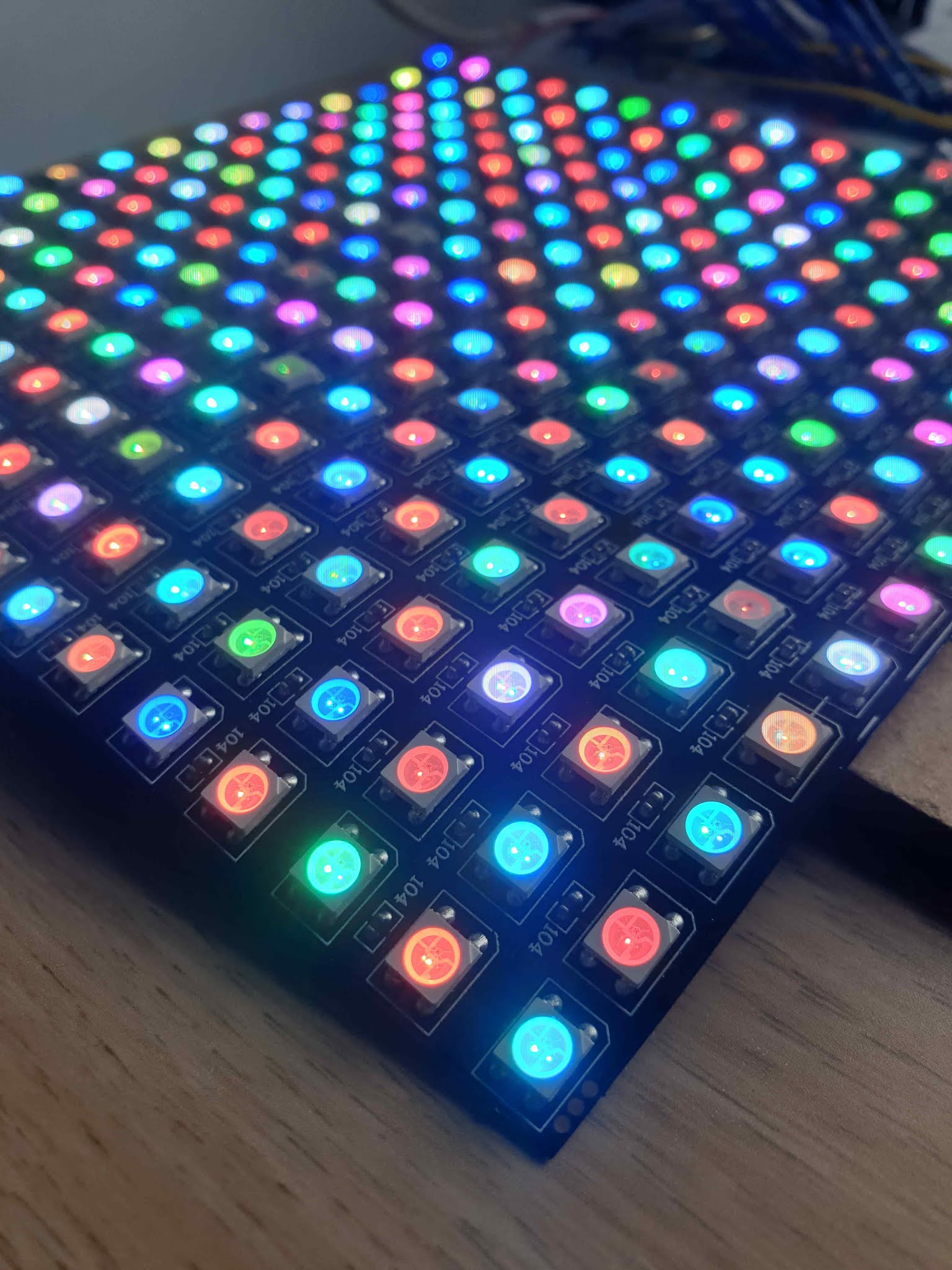
The LED strips need a suitable period of receiving no data in order to latch in the data they have received, i.e. a valid RESET signal. One approach could be to have this controlled by the 8-bit computer externally. I decided though to have the display updating constantly and provide some logic to disable the output... remember earlier when I said we could provide a signal to the final-NOR gate to do exactly this? This is where we'll use that now. Firstly, I had to finalise how many RGB LEDs I want to control... I settled on 256 LEDs, as this is a nice 16x16 matrix, or a 32x8 matrix. In terms of memory requirements this is 3 bytes per LED... 3 x 256 = 768 bytes. If we think about what is happening to the higher bits of the RAM address as we increment:
0-255 = 0x000 - 0x0FF = VALID MEMORY
256-511 = 0x100 - 0x1FF = VALID MEMORY
512-767 = 0x200 - 0x2FF = VALID MEMORY
768-1023=0x300 - 0x3FF = INVALID MEMORY, DISABLE OUTPUT
So if we switch off the NOR-gate output in the 0x300-0x3FF range, we can ensure we only send 768 bytes to the LED strip and also provide a long enough RESET signal. We need a function that outputs '0' for the valid memory and '1' for the invalid memory. We can get this trivially by taking the 8th and 9th bits of the memory address (i.e. '3': 8th bit = 1 and 9th bit = 1) and doing a logical AND with them! (in fact I use 2 NAND gates for reasons of having them on the board at the time of the 1st iteration, but the logic is the same).
I was excited to discover I could get some dual port SRAM, with 1024 bytes of 8-bit data quite cheaply, which means I can have one port dedicated to the LED display hardware and the second port connected to the 8-bit computer memory and data bus. The RAM I identified is called
IDT7130SA/LA (
datasheet) though it was not very available commercially. In the end I managed to find its bigger brother,
IDT7132SA on Ebay, which has 2k of dual-port SRAM, but is essentially the same beast.
Starting to put it together...
So far, I have tested this by using a slow clock, and some LEDs on the various clock and data output pins to test and all the timings seem to be working well. Now it's time to add a suitably fast clock and see what happens with a real LED strip...! I had a 2.4576 MHz clock on hand from my
UART transceiver module and in fact this gives the appropriate timing, about 400 ns per timing interval.
This is what the final schematic looks like (click to see a bigger version), with some annotations:
I have also
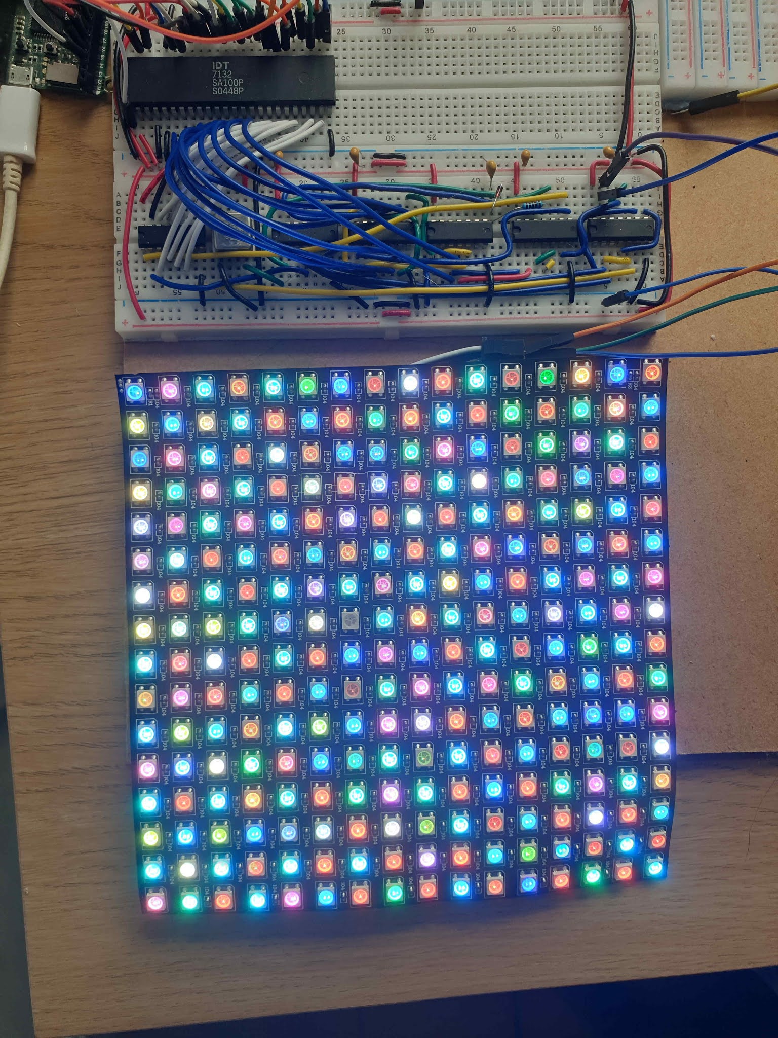
uploaded the schematic to Github. Wired together the board looks rather compact and I think pretty. I really like that it fits on a single breadboard (not including the RAM), making it truly modular and in the spirit of the breadboard computer.
The top board has the 2k 7132 DPRAM which will be joined later by a ROM memory chip and become the dedicated breadboard to host the CPU memory. The white wires are the data output from the DPRAM and the blue wires are the RAM address. From left to right, obscured partial by the blue address wires are the: 74LS165 shift register, 2.4576 MHz clock, 3 x 74LS393 counters, 74LS00 NAND and a 74LS02 NOR.
For the record, the time it takes to send each encoded bit of data is approximately 4 x 400 ns =1.6 us. Therefore an 8-bit byte is sent in 8 x 1.6 us = 12.8 us. The RAM streams 1024 bytes per display cycle, which will take approx. 13.1 milliseconds to send. The frames per second is therefore quite decent, at 76 fps, which corresponds to 76k per second. I have no doubt that the limiting step will be how fast my 8-bit computer can write to the other port of the RAM. As discussed, the reset signal for the WS2812 LEDs is provided by switching off the NOR-logic output during the "invalid" RAM address phase, and therefore lasts a quarter of the update time, i.e. 13.1 ms / 4 = 3.3 ms.
Testing - starting slow, 16 LEDs in a ring.
At the time of writing this section, I only have a 16 LED off-brand "Neopixel"-type ring which I *believe* has WS2812b LEDs, and I am waiting for my RAM chips and LED matrix displays to arrive. So using the 16-LED ring in the meantime, powering it up and plugging it into the LED data output and I get... a white light from the ring! This seems to make sense, as without the RAM memory attached, the shift register inputs will float high and the red, green and blue bytes will be all set to 0xFF. If I change some of the shift register inputs to GND manually, I can get the ring to get dimmer in a way that seems to make sense.
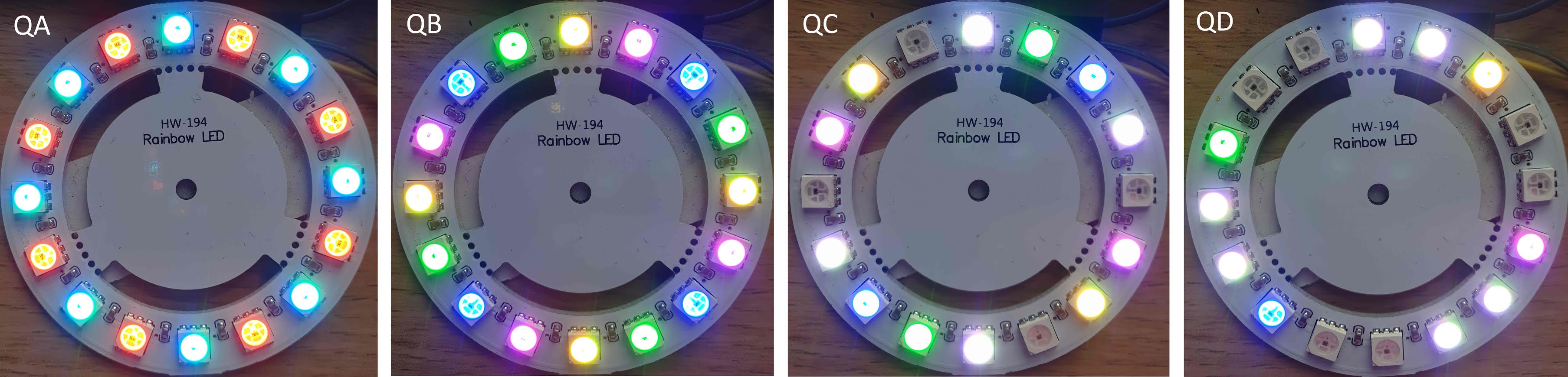
So far so good. How else can I test things? I had the idea to take the QA-QD outputs from the RAM address counter and use one as the data-bit input. This gave me four pretty and stable patterns as below:
This is certainly reassuring that *something* is happening! Does it make sense though? It turns out, YES it does. We can work out exactly what should be being sent and compare it to reality, for example for the QA and QB outputs:
I also completed this analysis for the QC and QD outputs, and confirmed that the colour patterns observed do indeed match reality. So the data appears to be being sent at a rate that the LED strip is happy with, and is correctly encoding 1s and 0s in a stable manner. The real test now will be putting data into the RAM and having it output onto the display correctly.
Putting data into the RAM
Excitingly, my RAM had now arrived and after hooking up the data lines and address lines to the board, my 16-LED ring showed some pretty colours! I think these colours are generated from whatever random values are in the RAM when it is powered up. Encouragingly, the LED colours are stable which makes me think my logic scheme is sound. I don't have the memory module of the 8-bit computer operational now, so how to write data into the RAM for testing? I thought about hooking up an Arduino, maybe one with lots of GPIO pins (i.e the Arduino Mega 2560), or a smaller Arduino with some shift registers, but I realised that I'd had a v1.0 pyboard sitting unused and lonely on my bench for a few years. These boards have a squillion of GPIO pins and use micropython scripts so couldn't be easier to interface with. I therefore hooked the unused port of the RAM up to the pyboard.
Above: The temporary installation of an v1.0 pyboard to write data to the RAM for testing
Now, I knocked together some Python code to write a specified byte at a specified address. Low and behold, it works! I was able to set any pixel to any colour and wanted, and had some fun cycling through RGB sine waves and mixing colours. I struggled to get a decent video (or indeed still photographs) of that, and I was also surprised by just how bright these LEDs are - like burn your retina bright. I also realised that I'm going to have to make an LED diffuser "pixel art"-type box for the 16x16 LED matrix that I plan to use this with as a simple sheet of tracing paper greatly improved the look of the NeoPixel ring in person, and made it much easier to photograph.
Not my best photograph, but you get the idea - we can now
individually address and control the colours of our NeoPixels!
Connecting the LED matrix/matrices
Almost there - now I needed to hook up my 16x16 WS1812b LED matrix to this module and see if it works. Clearly the connection is trivial and looks like this before powering up:

Switching it on, I was greeted with a pretty LED matrix. representing the random data that is in the RAM! First though we need to check that we haven't mixed up any of the data lines and that we can address the pixels in the expected way.
I wrote a bit of Python code to walk through each pixel and confirm that the addressing was working as expected. Not the most interesting video, but you can see what is happening here, I am writing 3 bytes of 255 to RAM (i.e. full R, G and B) so that every pixel is illuminated as white in order. Note that there is a delay between pixels which an intentional pause for 0.1 seconds.
With that working, I decided to write a quick python script to take a given image on my laptop (actually a list of images), then convert them to a bytearray in the required format for the RAM, taking into account the 'zig-zag' nature of the pixel order:
image_create.py.
I can then copy 'RAMimages.py' that is created onto the pyboard, import it and write those bytearrays to the RAM using the pyboard and running
main.py ... hey presto!
Left: A rainbow square image placed into RAM and right, the
Hackaday logo spat out of RAM in a TTL bitstream to be visualised.
Hardware double buffer
Remember how I wanted the 1k DPRAM but could only find the 2k DPRAM? I can of course use that extra 1k as regular RAM, but it struck me that I could display another image in that bank of RAM, like a hardware double buffer, and then switch between them to provide hardware animation or flicker-free display updates. The implementation is very straightforward. The address pin A10 on both the left and right ports of the DPRAM is currently tied to GND, but I can let the pyboard set it on the CPU side, to write an image either to 0x000 or 0x400 by setting A10 either low or high. Once that memory is written, I can direct the LED module to display either bank by setting A10 either low or high. At the moment this is controlled by the pyboard, but in the final computer this signal will controlled by an SR latch that the CPU can toggle between with an instruction. This approach really worked in a very straightforward manner to provide a 2-frame animation, below.

I also started playing around with a piece of 3 mm opal acrylic glass to help diffuse the image for taking pictures, and playing with some pixel art I found online.
Next steps and thoughts
Diffuser box: I think I want to make a "pixel art" LED diffuser box for my LED panel, to really make it zing. From other 16x16 projects I've seen, having a diffuser element with a grid inside can really sell the illusion of the LEDs as pixels. I think it makes sense to work on the memory and memory address registers next, to fill in this part of the CPU. I can imagine displaying something like Tetris, Pong, a cute 8-bit pixel art animation, representing prime number space, or as a RAM visualisation. In a nutshell I can definitely see some practical use for this in the final computer - which is good after all that effort!
Power: The current requirements for the panel, with every pixel on full is approximately 15A (by my calculations...) so I am surprised that the display looks so good when only powered from a USB port on my laptop. It is true not every pixel is on full, but still, I was pleasantly surprised. I do have a 5V, 20A power supply on standby, which I will no doubt migrate to using soon.
Baby: Having just had a baby, my hobbying (and sleep!) have really taken a hit, but what I like about this 8-bit computer project is that it is very modular, meaning I can work on a single module and integrate it. With the baby coming along I am getting stuck into dirty nappies/diapers and not sleeping (did I mention that already? Sleep deprived you understand), so progress has slowed, but crucially not stopped! I am a finisher by nature, even if finishing takes longer than anticipated.
Pyboard: Having this pyboard to hand with so many GPIOs pins was so useful. I can definitely see myself using this as a stand in for control logic (for example) and other places as the 8-bit computer is assembled. microPython is just so easy for quick hardware scripting, I am definitely a fan.
Reflections: It could be argued I got distracted by implementing this module (and my
UART transceiver) before getting my house in order with the basic CPU architecture. I suppose this is a classic case of pursuing the shiny fruit before sorting out the relatively "boring" basics. I will learn my lesson though, and I'll will sort out the program memory, ALU, MAR, SP and PC before thinking about other peripherals - no not even that Nintendo controller interface I have in mind. I must be strong.
Schematics and relevant python code is on
Github. Also the 8-bit computer now has a name -
Duncatron!
Please let me know of any questions or comments below


This comment has been removed by a blog administrator.
ReplyDeleteThis comment has been removed by a blog administrator.
ReplyDeleteThis comment has been removed by a blog administrator.
ReplyDeleteThis comment has been removed by the author.
ReplyDeleteThis comment has been removed by a blog administrator.
ReplyDeleteLooking at the schematic, there seems to be a small error, and maybe why you were having some problems. The reset circuit with R1 looks odd, normally you'd place the capacitor from clr input to ground and then connect the resistor to the end of the capacitor at the clr input (other end to the diode).
ReplyDeleteNice spot! The breadboard circuit is correct but the schematic as incorrect - updated now, thanks :)
DeleteAppreciate you blogging thiss
ReplyDeleteThis comment has been removed by a blog administrator.
ReplyDelete