MAR and memory
Memory Address Register (MAR) and Memory
Memory is (obviously) an essential part of a computer, and this blog post is part of a series and concerns adding different types of memory to my 8-bit computer.
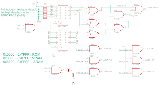
The memory of my 8-bit computer is addressed with a 16-bit address register, which gives access to 64k of memory. I have divided this memory space into ROM (EEPROM), VRAM (for the LED WS21812b module) and SRAM, with the following memory divisions:
0x0000-0x7FFF: ROM
0x8000-0x87FF: VRAM
0x8800-0xFFFF: SRAM
A zero-page in SRAM can be accessed at 0x8800-0x88FF. In terms of the electronics, this is achieved by not writing to the high databus (D8-D15), and instead letting a set of pull up and down resistors set the high databus to 0x88 by pulling D15 and D11 high, and D14-12 and D10-8 to ground. By not writing "0x88" explicitly to the high databus, instructions that access this memory are quicker than they otherwise would be.
The address decoding logic is fairly straightforward. The Memory Address Register (MAR) latches from the low (D0-7) and the high databus (D8-D15) with two 74LS574 flip-flops controlled by a "MI" (MAR 'in') ANDed with the system clock. And the addresses are decoded with OR (74LS32), NOR (74LS02) and AND (74LS08) logic. This produces an active-high signal for each memory segment (ROM, VRAM and SRAM) which is then NANDed (74LS00) with a clocked-control signal (RI = data in, RO=data out), to give active low output enable and write enable signals for the different memory ICs. The control signal for the write enable is pulsed through an RC network to give the required delay for writing the data.
The MAR register is indicated by the 2 blue LED bargraphs on the left hand side. The ICs in the above breadboard and to the left are used for the address decoding logic. The 3 large chips in the breadboard below from left to right are: VRAM (IDT7132SA, 2k x 8), SRAM (CY62256N, 32k x 8) and ROM (AT28C256. 32k x 8). Only the AT28C256 memory IC is hooked up to the MAR address and the databus in the image above. I later connected the rest of the ICs with ribbon cables.Testing
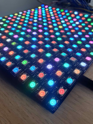
Connecting the 3 memory ICs to the 16-bit address bus and the databus was rather tedious, but it was made easier by making my own custom Dupont connectors. I hooked up my micropython pyboard to the low and high databus, the control signals and the clock to test writing and reading the data, using this script. Things seemed to working nicely! To test out whether each address could be uniquely accessed and written too, I decided to use random numbers to fill the banks of memory under test. As random numbers are not really random, but a sequence, by resetting the random seed before writing and reading, I could be sure to generate the same sequence twice. Satisfying, this worked really nicely and I was able to hook up an LED display and start writing values to it, via the high and low databus.
Conclusions
Things are starting to come together. Still on the list of things to implement, I need a program counter (PC), stack pointer (SP) and an Instruction Register (IR), among other things. The MAR is a significant milestone however and it is a relief to finally have it finished!
As always, the schematics and python testing scripts are available here on github. The evolving repository for the entire 8-bit computer project is here: Duncatron.


Comments
Post a Comment